


Kexin Electronics
PCB Drilling Routing Solutions Since 2006

 admin
admin  January 21,2026
PCB drilling is divided into through hole, blind hole and buried hole.
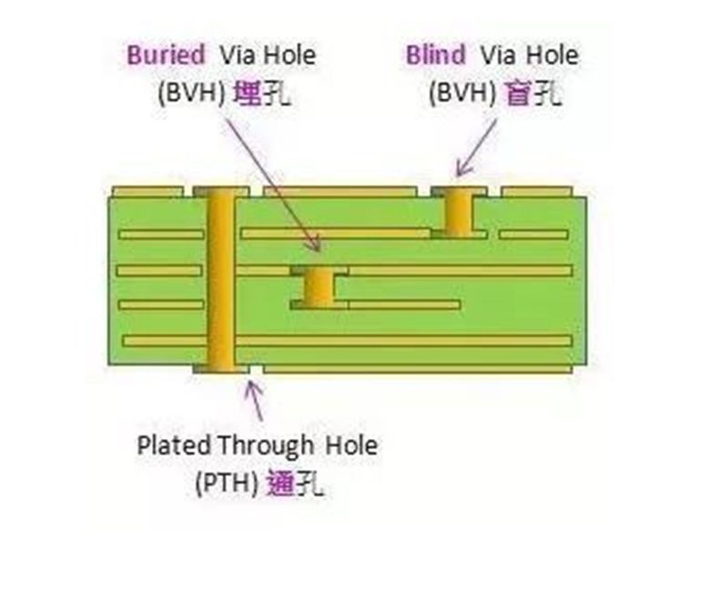
The copper foil circuit between the conductive patterns in different layers of the circuit board is conducted or connected by this kind of hole, but the copper plating hole of the component leading leg or other reinforcing materials cannot be inserted. Printed circuit board (PCB) is formed by stacking many copper foil layers. Because each layer of copper foil is covered with an insulating layer, they need to rely on via for signal link.
Technology of through hole
1. Only copper is needed in the hole, and the welding resistance can be plugged or not;
2. There must be tin lead in the hole, with a certain thickness requirement (4um), to avoid solder blocking ink entering the hole, resulting in tin beads in the hole;
3. The through-hole must be provided with solder stop ink plug hole, light tight, free of tin ring and bead, and must be flat.
Blind hole
It is to connect the outermost circuit in the printed circuit board (PCB) and the adjacent inner layer with electroplated holes. Because the opposite side cannot be seen, it is called blind through. In order to increase the space utilization between board and circuit layers, blind holes are used. The blind hole is a through hole to the surface of PCB
The blind hole is located on the top and bottom surface of the circuit board and has a certain depth. It is used for the connection between the surface circuit and the bottom inner circuit. Generally, the depth of the hole has a specified ratio (aperture). Special attention should be paid to this production method, and the drilling depth must be just right, otherwise it will cause electroplating difficulty in the hole. As a result, few factories will adopt this production method. In fact, it is possible to drill holes in the circuit layer to be connected in advance, and then glue them together. However, more precise positioning and alignment devices are needed
Buried hole
Connection between any circuit layers inside a printed circuit board (PCB), but not with the outer layer.
This production process can not be achieved by the way of drilling after the circuit board is bonded. It is necessary to drill at the time of individual circuit layers. First, the inner layer is partially bonded, then electroplated, and finally all are bonded. Because the operation process is more difficult than the original through-hole and blind hole, so the price is also the most expensive. This manufacturing process is usually only used for high-density circuit boards to increase the space utilization of other circuit layers.
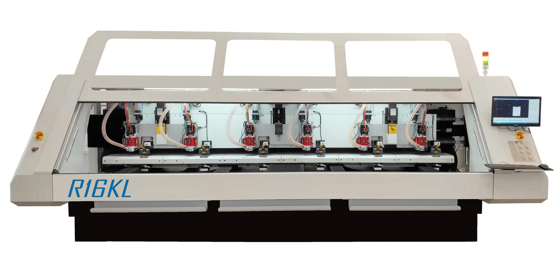
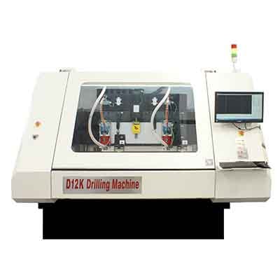
In the production process of printed circuit board (PCB), drilling is very important. The simple understanding of drilling is to drill the required through-hole on the copper clad plate, which has the function of providing electrical connection and fixing devices. If the operation is not correct and causes problems in the process of through-hole, the device cannot be fixed on the circuit board, which will affect the use of the circuit board in light and the whole board will be scrapped in heavy, so the process of drilling is quite important.


![$siteconfigs['company_email']}](/res/baiila/images/home/emi.png)
